
- Home
- Products
- Solutions
- About
- Service
- Sustainability
- News
- Contact Us

Views: 0 Author: Site Editor Publish Time: 2026-10-15 Origin: Site


As semiconductor node sizes shrink, the tolerance for particulate and chemical contamination in the fabrication environment drops to near zero. Standard industrial graphite outgasses impurities like vanadium, iron, and boron at extreme temperatures. These trace metals lead to lattice defects, altered electrical resistivity in silicon wafers, and catastrophic yield losses.
Selecting the right semiconductor graphite requires matching the exact thermal, chemical, and purity profile of the material to the specific fabrication process. This guide breaks down how high-heat and chemical environments dictate purity baselines. We will also explore how you can evaluate suppliers for mission-critical components. You cannot afford to treat these materials as generic commodities. Every heating cycle tests the structural limits of your fixtures. By understanding the rigorous demands of advanced nodes, you protect your production yields. Let us dive into the technical benchmarks defining these ultra-pure materials.
Microscopic trace metals migrating from fixtures into a silicon melt or epitaxial layer cause immediate structural defects. These defects invariably lead to electrical failure. A single migrating metal ion can ruin an entire wafer batch. When you heat standard graphite, it releases trapped elements from its porous structure. Iron and vanadium act as deep-level impurities in silicon. They degrade minority carrier lifetime. Boron and phosphorus act as unintentional dopants. They shift the electrical resistivity unpredictably. You lose control over the fundamental properties of the wafer.
High operating temperatures in vacuum or inert gas environments multiply these outgassing risks. Extreme heat forces volatile ash and elemental impurities out of the unpurified carbon matrix. In a vacuum, vapor pressure dynamics accelerate this release. The outgassed elements then deposit directly onto the sensitive silicon substrate. They form micro-clusters. These clusters disrupt the crystalline lattice. Yield rates plummet when these atomic-level disruptions occur. You must prevent this migration at the source.
To combat this, manufacturers rely on strict baseline ash content metrics. Ash content represents the total volume of inorganic impurities remaining after carbon combustion. Standard industrial graphite might contain hundreds of parts per million (ppm) of ash. Semiconductor fabrication cannot tolerate this. For advanced nodes, total ash content must routinely fall below 5 ppm. Many mission-critical applications demand levels below 1 ppm. Specific elemental limits plunge even further into the parts per billion (ppb) range.
Common mistakes in baseline purity assessment include:
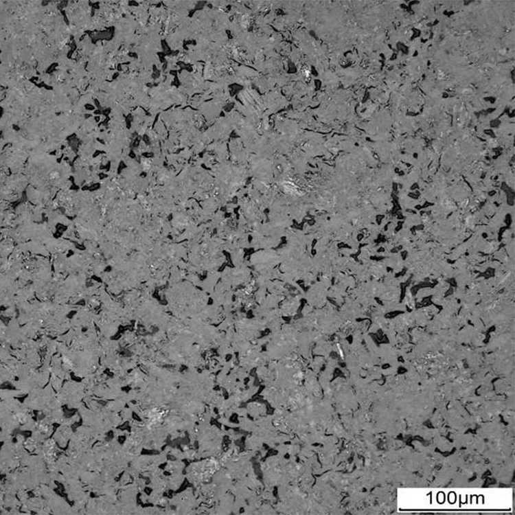
Different manufacturing stages expose tooling to unique thermal, chemical, and physical stresses. You must align the material properties to the exact process environment.
Table 1: Graphite Material Requirements by Semiconductor Process
| Fabrication Process | Core Components | Purity Baseline | Primary Engineering Challenge |
|---|---|---|---|
| Czochralski (CZ) Growth | Crucibles, heaters, heat shields | < 5 ppm (Zero Group III/V) | Prolonged exposure to molten silicon at ~1450°C |
| Epitaxy (MOCVD) | Susceptors, wafer carriers | < 1 ppm (Often SiC coated) | Preventing direct surface defects on crystalline layers |
| Ion Implantation | Beam stops, arc chambers | < 2 ppm | Resisting high-energy ion bombardment and sputtering |
The Czochralski process creates the foundation of the semiconductor industry: the monocrystalline silicon ingot. Components like crucibles, heaters, and heat shields face extreme conditions. They are exposed to molten silicon at approximately 1450°C for extended durations. This process reality demands absolute thermal stability. Structural degradation here destroys a massive volume of costly material.
The core requirement is a zero-tolerance policy for Group III and Group V elements. Elements like boron and phosphorus act as unintentional dopants. If they leach into the silicon melt, they permanently alter the electrical characteristics of the ingot. Furthermore, the material requires exceptional thermal shock resistance. Large temperature gradients occur as the ingot pulls away from the melt. Any micro-cracking in the heater elements will generate catastrophic particulate contamination.
Epitaxial processes demand an entirely different approach. Susceptors hold wafers firmly while reactive gases deposit crystalline layers across the surface. The process reality involves highly corrosive precursor gases reacting at elevated temperatures. The graphite cannot interact chemically with these gases.
This requirement necessitates ultra-low porosity and uncompromised surface integrity. Impurities in this chamber cause direct surface defects on the wafer, destroying the active device regions. To survive this, engineers often rely on specialized coatings. You will frequently see SiC-coated graphite used here. The coating seals the porous carbon network. It prevents residual impurities from outgassing and protects the core material from corrosive attack.
Ion implantation introduces dopants into the wafer via high-energy ion bombardment. The process reality is brutal. This bombardment causes rapid physical wear. It creates potential sputtering of the graphite components. The tooling takes direct hits from energized particles.
The dominant requirement shifts toward mechanical durability. High mechanical strength and an ultra-fine grain size become mandatory. The material must resist erosion aggressively. If the surface erodes unevenly, the graphite itself becomes a particulate contaminant. Loose carbon dust in an ion implanter causes severe arcing and electrical shorting across the wafer.
Standard carbon materials exhibit directional properties based on their manufacturing method. This directional variance causes fatal issues in wafer processing. Isostatic pressing solves this problem by applying equal pressure from all directions during forming.
You must contrast anisotropic (extruded or molded) graphite against isostatically pressed variants. Extruded materials expand at different rates depending on the grain orientation. This unequal expansion causes warping. When you heat an extruded susceptor, it bends. A bending susceptor creates uneven heat distribution across the wafer, ruining the deposition process. Uniform, non-directional properties prevent this uneven thermal expansion. This makes isotropic graphite for semiconductor applications the undisputed standard for maintaining tight geometric tolerances during rapid heating and cooling cycles.
Surface coatings amplify the need for isotropic structures. Consider the Coefficient of Thermal Expansion (CTE). You must match the CTE of the base graphite precisely to the CTE of the surface coating, such as Silicon Carbide (SiC). During thermal cycling, the component heats and cools repeatedly. If the base material expands faster than the coating, the coating stretches and breaks. This CTE mismatch causes delamination. Micro-cracking ensues. Subsequent particle shedding destroys the cleanroom environment. Isotropic materials provide a stable, predictable expansion rate across all three axes, keeping the protective coating perfectly intact.
Grain size and density dictate the final performance of the component. Finer grain sizes, typically below 20 microns, provide substantial benefits. They contribute to a significantly smoother surface finish. A smooth surface reduces the risk of particulate shedding. Furthermore, a smaller grain structure increases the overall density of the part. Higher density yields lower permeability. Corrosive gases struggle to penetrate a dense material. This directly extends the component's lifespan and maintains chamber cleanliness over hundreds of production cycles.
Best practices for evaluating structural properties:
Producing raw material is only the first phase. Shaping it into precise operational tooling requires exceptional engineering control. You face an inherent conflict between the material's brittleness and the required micro-tolerances.
Graphite machines beautifully, but it chips easily. Addressing the engineering challenge of shaping a highly brittle material requires specialized tooling strategies. You need micro-tolerances for semiconductor tooling to ensure perfect wafer contact. Poor contact causes uneven heating. Uneven heating causes wafer slip and dislocation defects. Machinists use advanced CNC centers operating at high RPMs. They employ specialized diamond-coated end mills to prevent edge chipping. They must control the feed rates meticulously to achieve a mirror-like surface finish without inducing subsurface micro-fractures.
Contamination during this shaping phase poses a massive hidden risk. High-purity blocks enter the machine shop clean. They often leave contaminated. Standard machine shops process various metals like copper, steel, and aluminum. The dust from these metals settles onto the graphite. The cutting tools themselves wear down, embedding iron or tungsten into the carbon surface. You must mitigate the risk of cross-contamination. Ensure the manufacturer uses dedicated, cleanroom-equivalent machining centers exclusively for high-purity grades. Semiconductor graphite machining requires an isolated environment to preserve the pristine nature of the raw block.
Even in dedicated facilities, some tool wear remains inevitable. This mandates rigorous post-machining purification. You cannot rely on pre-machined purity levels. High-temperature halogen purification must occur after the machining process. The finished parts enter a specialized furnace. They are heated to temperatures exceeding 2000°C. Technicians inject halogen gases, typically chlorine and fluorine, into the chamber. These gases react violently with any metallic impurities introduced by cutting tools. The reactions form volatile metal halides. These halides vaporize and are pumped out of the chamber. This final step guarantees the finished component meets parts-per-billion purity standards.
Selecting a supplier dictates your long-term yield stability. Marketing claims of "high purity" hold no value in a cleanroom. You need verifiable, scientific evidence backing every component.
When shortlisting vendors for low impurity graphite components, demand strict metrology and testing standards. Advise buyers to look for suppliers utilizing advanced spectroscopy. Glow Discharge Mass Spectrometry (GDMS) and Inductively Coupled Plasma Mass Spectrometry (ICP-MS) represent the gold standards. These techniques verify elemental purity down to the parts per billion (ppb) level. Ensure the vendor aligns their testing methodologies with NIST (National Institute of Standards and Technology) or equivalent international material standards. Transparent metrology reports prove the supplier actually measures what they claim to control.
Batch-to-batch consistency separates competent suppliers from dangerous ones. A single inconsistent batch can jeopardize an entire semiconductor production run. Focus on vertical integration. Does the supplier control the raw coke sourcing, the graphitization, the machining, and the final purification? Highly integrated suppliers maintain tighter quality control. If they outsource the final purification, your risk multiplies. Request historical statistical process control (SPC) data to verify their long-term consistency.
Follow this numbered process for vendor validation:
Finally, evaluate their capacity for application-specific customization. Process environments vary wildly between fabs. Assess whether the supplier offers active consultation on material grade selection. Do they provide specific coating recommendations based on your unique thermal and chemical environment? A true partner analyzes your exact process gases and peak temperatures. They then engineer a component designed specifically to survive those conditions, rather than pushing a catalog standard.
Semiconductor graphite is not a commodity. It functions as a highly engineered variable within the complex fabrication ecosystem. Process environments dictate absolute limits on thermal stability and trace impurities. From the molten crucible of Czochralski growth to the plasma-rich environment of an ion implanter, matching the material properties to the process saves yields. Isotropic structures ensure uniform expansion. Precision machining guarantees perfect fit. Rigorous halogen purification eliminates fatal trace metals.
You must take active control of your supply chain. We encourage technical buyers and engineers to audit their current component lifespan immediately. Look for signs of premature erosion or unexplained particle spikes. Request detailed ash-content breakdowns and CTE data sheets from potential vendors. Compare these against your process parameters. Initiate pilot testing for mission-critical parts to validate supplier claims under actual cleanroom conditions. Proper material selection minimizes downtime and protects your bottom line.
A: Typically, the maximum allowable ash content sits below 5 ppm. However, advanced applications demand stricter limits. Many modern processes require total ash below 1-2 ppm. Furthermore, they enforce ppb-level limits for specific transition metals like iron, copper, and vanadium to prevent yield losses.
A: Isotropic materials exhibit uniform thermal expansion across all directions. This non-directional property prevents warping during rapid heating cycles. Extruded materials expand unevenly, which bends the component and causes uneven wafer heating. Isotropic grain structures guarantee structural stability and precise dimensional control.
A: Yes, it significantly affects purity. Tooling wear introduces contaminants directly into the material's surface. Cutting tools shed microscopic amounts of iron or tungsten. Therefore, manufacturers must perform stringent post-machining halogen gas purification at extreme temperatures to vaporize and remove these embedded trace metals.
A: A Silicon Carbide (SiC) coating seals the porous graphite network. It prevents particle generation and stops the outgassing of any residual impurities. Additionally, it protects the base graphite from corrosive process gases, extending the component's operational lifespan in aggressive epitaxy or CVD environments.


